Radiation damage in nanoporus nuclear materials
The performance of plasma-facing materials used in the extreme environments of irradiation and heat load must be significantly improved to extend the reliability, life-time, and efficiency of future nuclear fusion reactors. Under irradiation, defect clusters can nucleate and grow by absorption of point defects (i.e. vacancies or interstitials). In addition, during neutron-induced transmutations, helium may be generated via n,α reactions and in the absence of a means of escape (referred to as a “sink”) they can become trapped in regions of low electron density such as vacancies and grain boundaries. This can lead to the formation of small bubbles of helium gas. This can result in embrittlement and dimensional instability of irradiated materials. Therefore, the ability to remove radiation-induced point defects and control helium bubble nucleation and growth are crucial to improving the mechanical properties of components in a nuclear reactor. This challenge calls for novel approaches to designing materials that resist radiation damage while maintaining high strength and toughness.
Nanoporous materials have recently attracted attention as potential materials for nuclear applications. They have incredibly large surface-area-to-volume ratios which provide a high-density of sinks for the annihilation of defects and gas bubbles. We are currently using nanoparticles and nanowires to represent the nanoporous ligament structure. We are investigating various model systems including tungsten, molybdenum, silicon carbide and iron which represent those considered as potential plasma-facing materials in the International Thermonuclear Experimental Reactor (ITER) and DEMOstration fusion power plant as well as for components in Generation IV fission reactors. Ion irradiation experiments are carried out at the Microscopes and Ion Accelerators for Materials Investigations (MIAMI) facilities to introduce radiation damage using helium and self-ions whilst observing the dynamic effects on these materials.
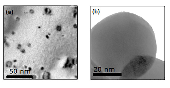 Transmission electron microscopy images of (a) bulk tungsten and (b) tungsten nanoparticles
The above shows transmission electron microscopy images of (a) bulk tungsten and (b) tungsten nanoparticles both irradiated with 15 keV He ions at 750°C showing an accumulation of dislocation loops in the bulk whilst there is no presence of dislocation loops in the nanoparticle indicating a greater tolerance to radiation damage accumulation.